Please support the Ministry’s public relations work: We need your consent to be able to measure your user activity on our website using etracker. A pseudonymised evaluation of this data by etracker helps us to improve our website. You can revoke your consent at any time for the future. Once you have made your selection, the consent management screen will appear at the bottom of the page. You can use this to stop or to reactivate the statistical evaluation at any point. You can reactivate tracking by dragging the slider in the opposite direction.
This website sets temporary session cookies. These are strictly necessary and therefore cannot be deselected. Their sole purpose is to enable you to use the website.
The Ministry also presents its work on this website in the form of videos. These are made available by the provider TV1 using JW Player. Please consent to the transmission of your IP address and other technical data to JW Player and allow JW Player to set cookies on your end device if you wish to view videos on our website. We also provide a consent management function for this at the bottom of the page. You can use this to control whether JW Player is enabled or not.
You can find detailed information on your rights and how we protect your privacy in our privacy policy.
Consent to the use of JW Player for video streaming
The Ministry also presents its work on this website in the form of videos. These are made available by the provider TV1 using JW Player. Please consent to the transmission of your IP address and other technical data to JW Player and allow JW Player to set cookies on your end device if you wish to view videos on our website. We also provide a consent management function for this at the bottom of the page. You can use this to control whether JW Player is enabled or not.
Everyone needs electricity and heat – but how to best organise transmission, distribution and storage? Go ahead and learn about the most intelligent designs and solutions!
Energy efficiency is key, both for the current building stock and for everything to be built from now on. Find out more about how the building stock can be made fit for future energy savings!
In tomorrow’s energy world, industries, commerce and agriculture use only a fraction of the energy they use today – with no negative effects on output.
Electromobility and new, alternative fuels are about to fundamentally change the transport sector. Find out more about the characteristics and prospects of these technologies!
In order to achieve an integrated energy system, power, heat and mobility need to be combined in a way that is both intelligent and sustainable. Take a look at relevant approaches in this field!
Are you looking for face-to-face meetings with German companies? Would you like to receive first-hand information? The German energy solutions initiative offers you a number of different possibilities to do so.
Sign up to our newsletter service to receive the latest information about German energy solutions and about opportunities to meet German business partners around the world.
All events
If you are interested in attending an event of the German energy solutions initiative, you will find the dates and locations in our calendar.
Increasing energy efficiency in soldering processes
Introduction
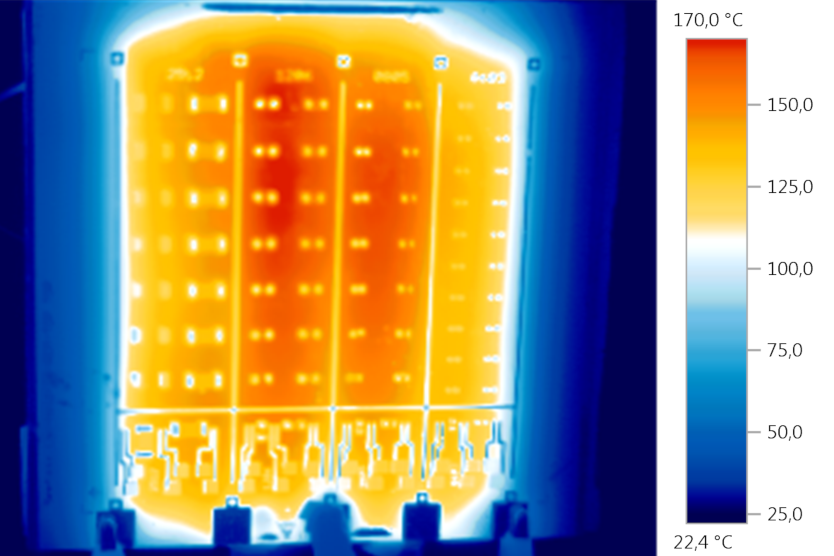
A research project is seeking an innovative way of substantially reducing the high-energy consumption in industrial soldering processes: the heat required for this is to be generated by the circuit carriers themselves.
The energy expenditure in standard convection reflow soldering processes for the industrial manufacturing of electronic assemblies is enormous, yet most of the heat produced in this process is not used: 99,8% of the heat is not produced by the solder paste deposits but by the assemblies themselves or is released into the furnace.
The partners of the research project “Energy and resource-efficient manufactured electronic assemblies (ERFEB)” are seeking to increase the low energy efficiency by integrating heating systems in the circuit carriers. A heating layer over the complete surface is to be embedded in the circuit carrier and is to generate the required heat in the areas it is needed via Joule heating. In theory, the potential savings in energy is 50%. In addition, there are savings in the nitrogen supply and in the surface area needed for the system. However, the heating layer should not only be available for use during the manufacturing process, but also in the subsequent operation of the assemblies and, for example, drying varnishes and condensate or to achieve certain operating temperatures.
In the course of the project initiated at the end of 2017, different materials will be tested and developed with regard to their suitability as a heating layer. Manufacturing tests will be carried out and other areas investigated that might be suitable for application apart from soldering.
The project that is to run for three years is being funded by the Federal Ministry for Economic Affairs and Energy (BMWi) and coordinated by Siemens Corporate Technologies. Apart from the University of Rostock and Neue Materialien Bayreuth GmbH, B & B Sachsenelektronik GmbH, Heraeus Deutschland GmbH & Co. KG and SEHO Systems GmbH are also among the project partners.
More information
Project information on the homepage of the University of Rostock
![Logo [EN]German Energy Solutions](/SiteGlobals/GES/StyleBundles/Bilder/sublogo_en.svg?__blob=normal&v=1 "To homepage")